

Retired hardware engineer [Plasmode] recently took on the challenge of building a debugger for the 6502 designed to sit atop the microprocessor while seated in a solder less breadboard. The result is the Diagnostic Overlay for W65C02 Breadboard, consisting of 128 kB SRAM and a 1250-gate CPLD. Except being 0.8 in wide, the overlay debugger is otherwise the same size as the 6502’s 40-pin DIP package, so it doesn’t overhang other portions of your circuit.
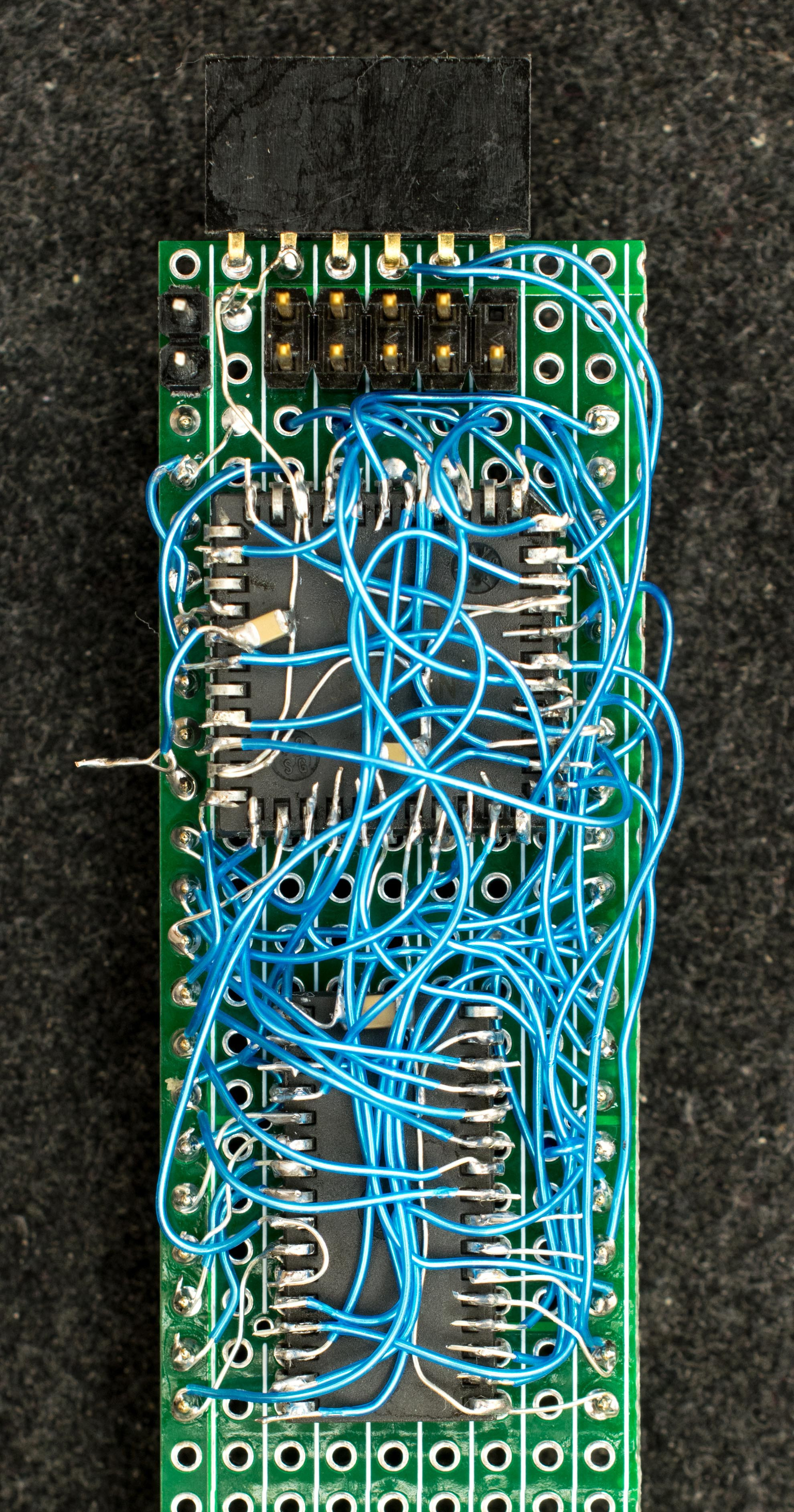
Being an initial concept prototype, [Plasmode] mounted the chips dead-bug style on perf board — a process he himself found tiring. If he builds additional debuggers, presumably he will consider making a PCB.
The prototype was constructed using point-to-point soldering with 30-ga wire wrap wire. It was all done under the inspection microscope. There are not many connections, but they are rather tedious so I can only do a dozen or so wires per session. It took me 2 days and several hours total to finish the prototype board.
This design is based on the CRC65 Frugal 6502 Single Board Computer, of course omitting the 6502 itself. Instead of a physical ROM memory chip, he implemented a 64-byte boot loader inside the CPLD and a serial port. This lets him to bootstrap the system over the serial port. He plans on expanding this to include other DIP-packaged retro microprocessors in the future. Check out his Hackaday.io project page ( above ). If you want to dig deeper, he posted the schematics here.
Support the originator by clicking the read the rest link below.


