

It seems only appropriate that hot on the heels of the conclusion of Hackaday’s 555 Timer Contest that [Ken Shirriff] posts a silicon die teardown of an early version of a hacker’s favorite chip, the 555.
A Microscopic View Of the 555 Die
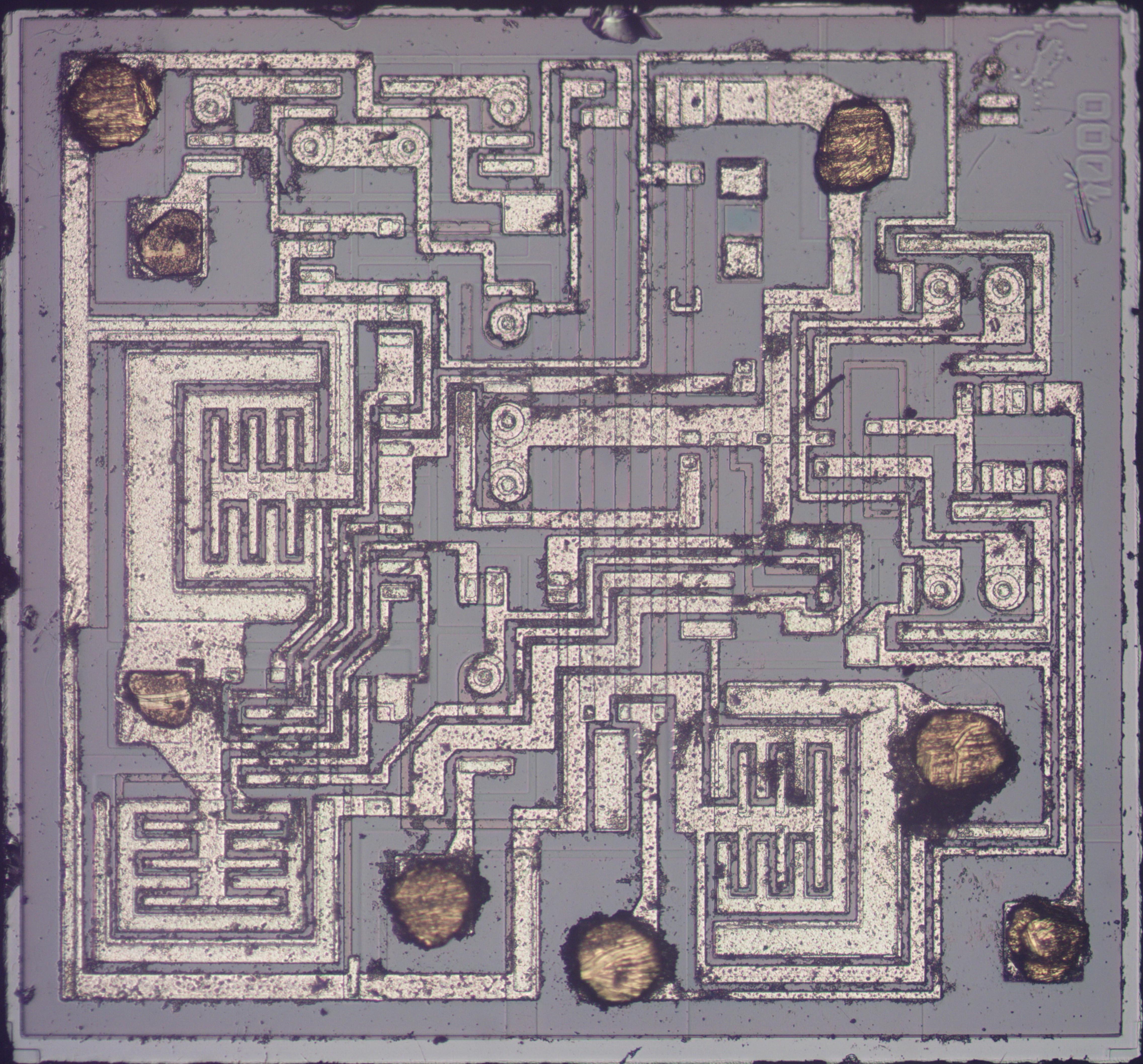
Starting with a mystery chip from January 1973, [Eric Schlaepfer] painstakingly sanded down the package to reveal the die, which he deemed to be a 555 timer. Why didn’t they know it was a 555 timer to start? Because the package was not marked with “555” but rather some other marks that you can see in the blog post.
In addition to a great explanation of how the 555 works in general, [Ken] has taken a microscopic look at the 555 die itself. The schematic of a 555 is easily available, and [Ken] identifies not just sections of the die but individual components. He goes further yet by explaining how the PNP and NPN resistors are constructed in silicon. There’s also a nice and juicy bit of insight into the resistors in the IC, but we won’t spoil it here.
Be sure to show your love for the winners of the 555 contest, or at the very least check out the project that took the stop spot: a giant sized 555 that you don’t need a microscope to see inside of.
Support the originator by clicking the read the rest link below.


